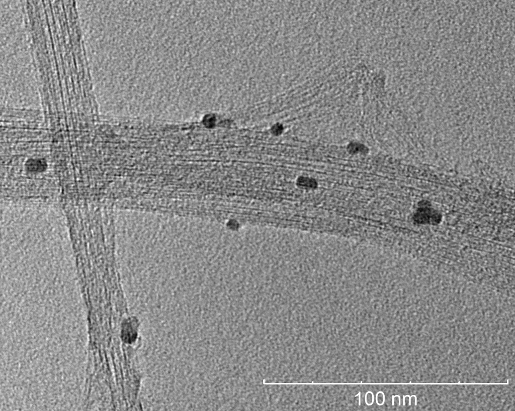
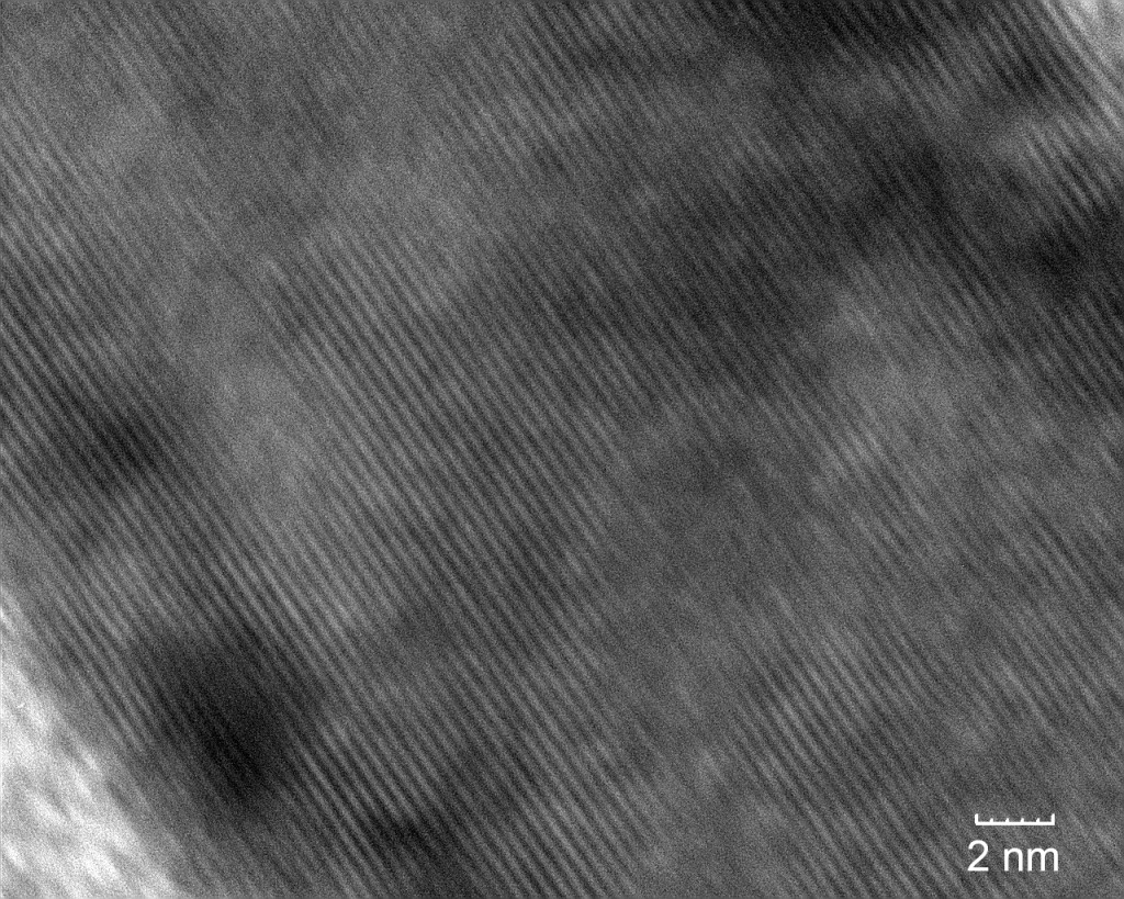
One of the current trends in materials science is to make materials lighter, stronger and more durable. Development and advancements in nanotechnology and nanomaterials are helping make progress towards that goal. New materials need to go through rigorous research and characterization to fully understand their properties. High resolution transmission electron microscopy is a great way to characterize new advanced materials. High resolution TEM imaging is TEM that allows for direct imaging of atomic structure of a sample. High resolution TEM imaging can attain spatial resolution in the 0.5 Angstrom range. With such high resolving power, HRTEM is an excellent technique for characterizing semiconductors, nanoparticles, and other advanced materials. The information obtained from a high resolution TEM is useful for studying atomic structure, lattice spacing, crystal symmetry, defects, surface structure and dislocations.
This webinar will discuss nano-scale structures and nanomaterials that can be imaged and characterized by HRTEM.
Speaker Bio
 Jake Spry is a Research Scientist at MVA Scientific Consultants specializing in analysis of micro- and nano-scale particles utilizing transmission electron microscopy (TEM) with selected area electron diffraction (SAED) and energy-dispersive X-ray spectroscopy (EDS). Jake also has training in analysis techniques with polarized light microscopy (PLM) and scanning electron microscopy (SEM).


