Expand Your Knowledge
Our resource center archives our case studies, published articles, blogs, webinars, and image galleries. Discover ways microscopy has made a meaningful impact.
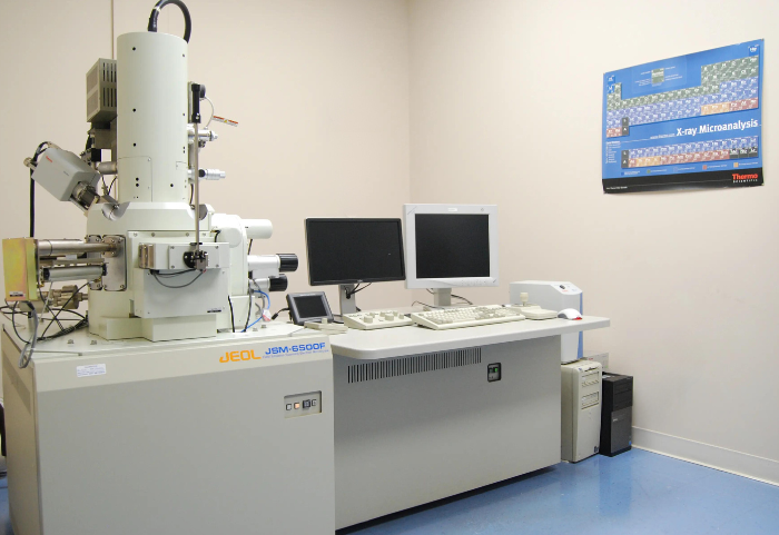
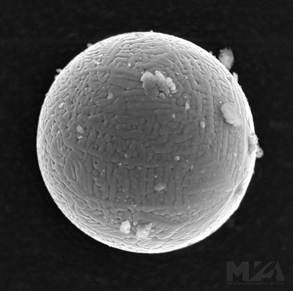
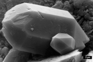
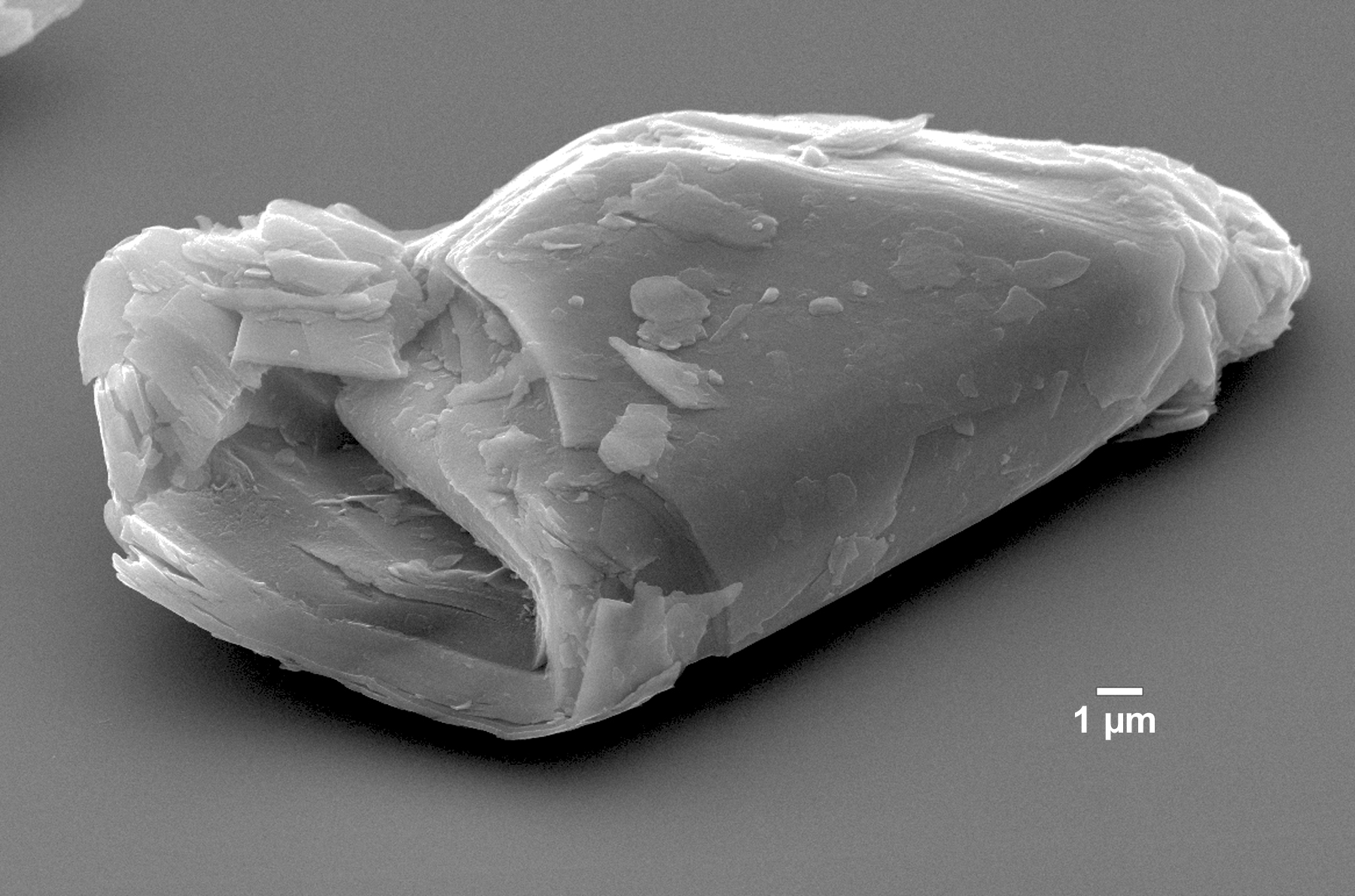
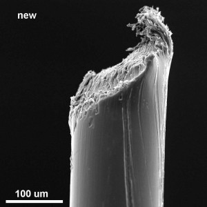
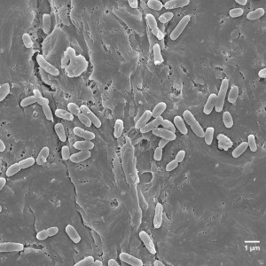
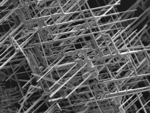
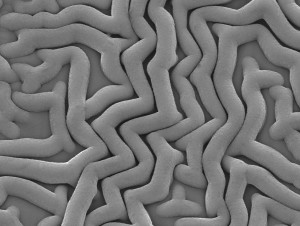
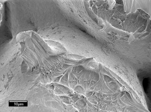
Scanning electron microscopy (SEM) allows us to examine and characterize particles and nanoparticles, fracture surfaces, surface morphologies, composites and their constituents, and microstructures of prepared cross-sections. The scanning electron microscope is one of the most powerful and useful tools for material analysis; it uses electrons rather than light waves to examine surfaces, permitting much greater magnification, resolving power and depth of field. SEM analysis provides us with high resolution imaging at magnifications up to 300,000X.
With the addition of energy dispersive x-ray spectrometry (EDS), we can simultaneously determine the elemental composition and morphology of different materials.
The field emission scanning electron microscope is configured similarly to a conventional scanning electron microscope, except that a field emission electron source is used, allowing higher resolution imaging, increased signal to noise ratio, and increased depth of field.
A field emission electron source produces electrons by applying a high voltage to a very sharp point and extracting the electrons directly and only from the point. The coherence and very small diameter of this source increases the useful magnification of the SEM by a factor of ten.
Our focus is to offer value and high quality data in a timely manner. Our SEM lab services offer a variety of customized analyses to clients with advanced materials across a wide spectrum of industries and applications, including:
Scanning electron microscopy with energy dispersive x-ray spectroscopy, also known as SEM-EDS, is considered a non-destructive micro-analytical technique, and it is effective for major and minor element analysis. The ability to characterize and identify small particles and other materials in the SEM is greatly enhanced by the common addition of EDS capability.
In the scanning electron microscope, the bombardment by the energetic electron beam induces the emission of x-rays at energies which are characteristic of the elements present in the sample. These x-rays are collected by an EDS detector, sorted and counted, and the result can be presented as an EDS spectrum or histogram. EDS can also produce an elemental map, which is an image of an area on a sample that shows the elements present and their concentration.
For more information, please contact us at 770-662-8509 or info@mvainc.com.