SEM/EDS Lab Services
Scanning electron microscopy with energy dispersive X-ray spectroscopy, also known as SEM/EDS, is considered a non-destructive micro-analytical technique, and it is effective for major and minor element analysis. The scanning electron microscope (SEM) is uniquely capable of providing high-resolution imaging (at magnifications up to 300,000X) of a sample surface structure for microanalysis and particle characterization. The ability to characterize and identify small particles and other materials in the SEM is greatly enhanced by the common addition of EDS capability.
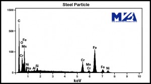
In the SEM the bombardment by the energetic electron beam induces the emission of x-rays at energies which are characteristic of the elements present in the sample. These x-rays are collected by an EDS detector, sorted and counted, and the result can be presented as an EDS spectrum or histogram. EDS can also produce an elemental map, which is an an image of an area on a sample that shows the elements present and their concentration.
Our focus is to offer value and high quality data in a timely manner. Our SEM lab services offer a variety of customized analyses to clients with advanced materials across a wide spectrum of industries, including:
- Pharmaceuticals
- Medical devices
- Cosmetic products
- Food manufacturers
- Environmental
- Semiconductors
- Polymers
- Coating
- Nanoparticles and nanotubes
- Glass containers
- Minerals
- Failure analysis
Contact us at 770-662-8509 or info@mvainc.com to learn more about how we can use the SEM to answer your specific analysis and testing needs.
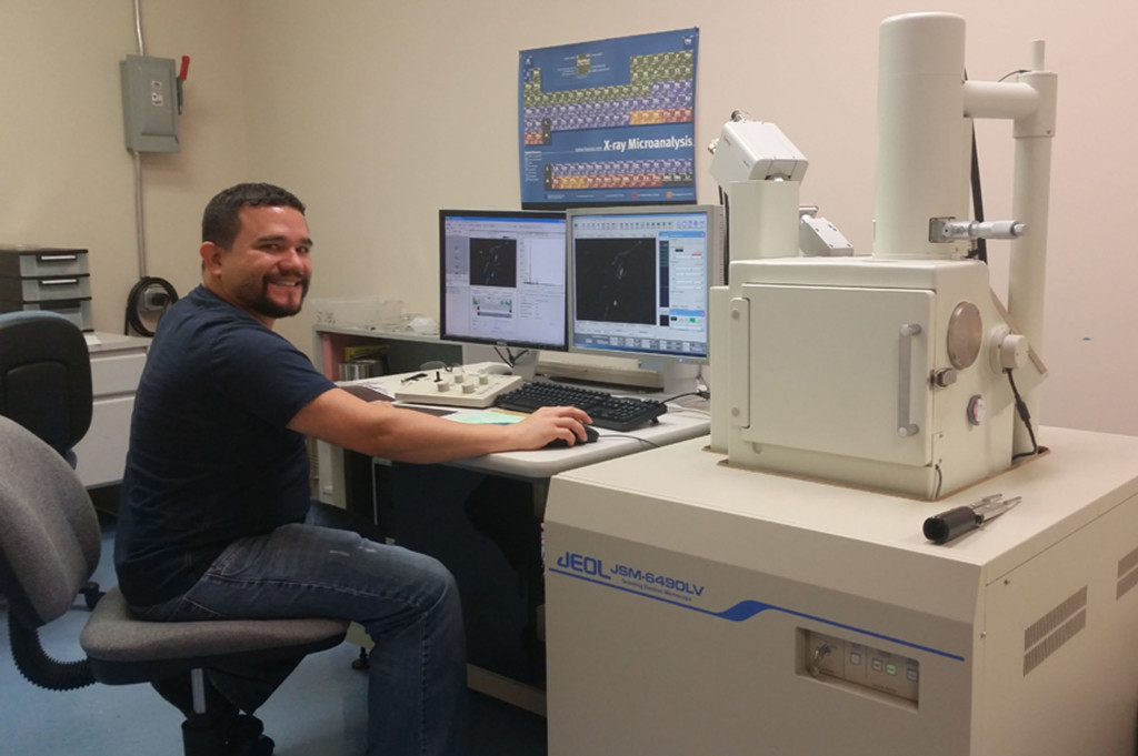
This Low Vacuum SEM includes a variable pressure system capable of holding wet
and/or non-conductive samples with minimal preparation. The large sample chamber allows the analysis of a wide variety of sample types and sizes.
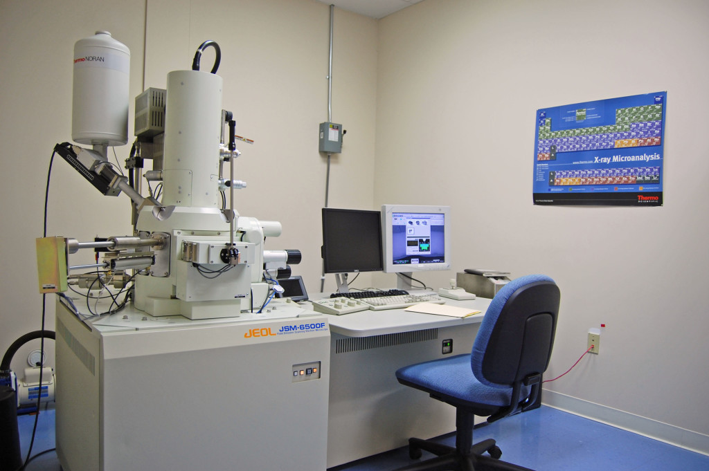
This Field Emission SEM provides high-resolution imaging during SEM analysis
at magnifications from 5x to 300,000x.


